Nokia Booklet
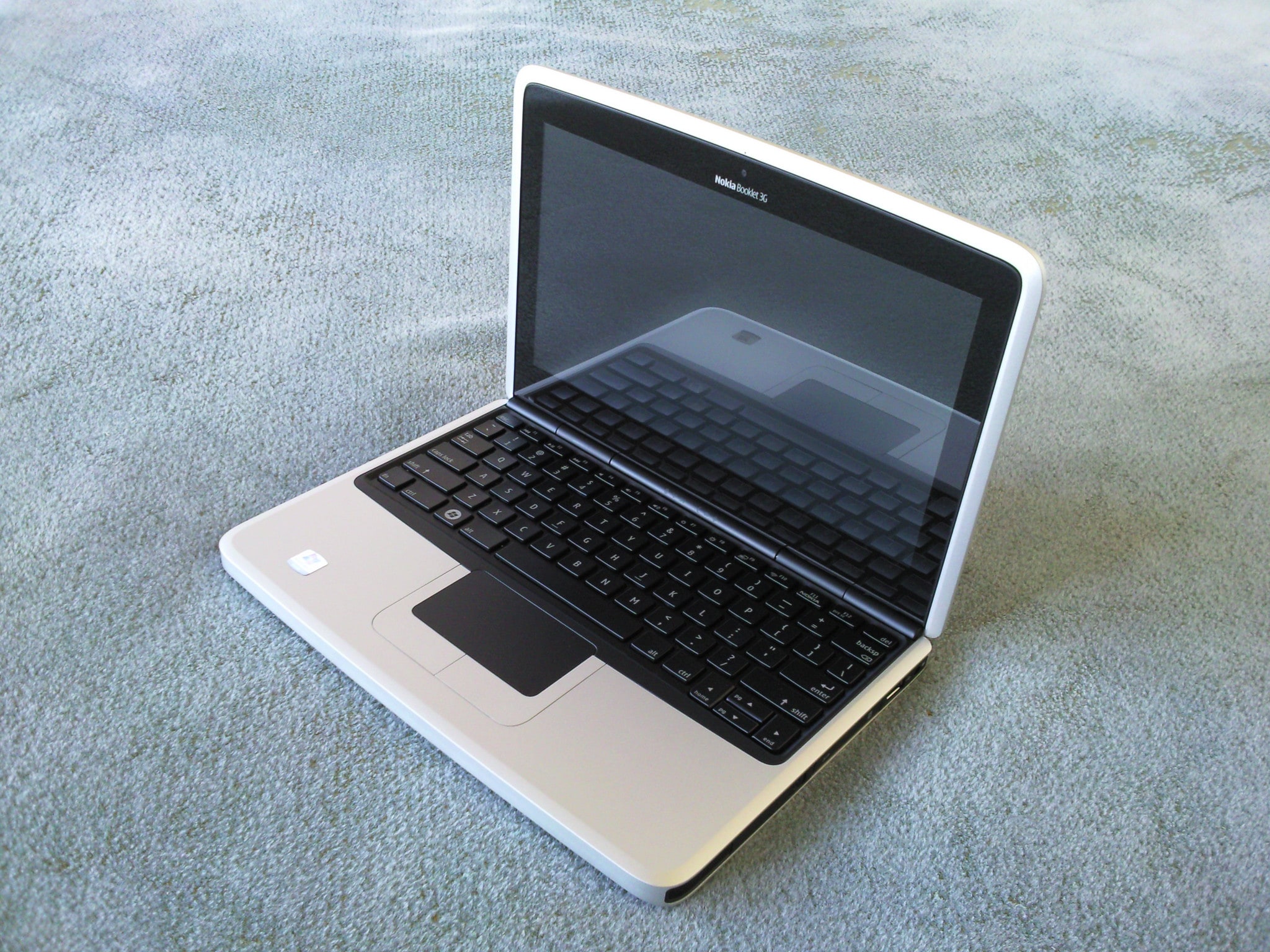
The Nokia Booklet 3G is a netbook made by Nokia, a Finnish telecommunications company. Nokia announced the machine on 24 August 2009. It was the company's first netbook.
The production model is NYU00. Compal and Tripod made the machine for Nokia. Its platform uses Intel's Menlow design, with an Atom Z530 processor and an SCH US15W chipset.
This document describes the hardware, firmware, internal connections, and operating system interfaces of the Booklet 3G. It also records findings from Rime, a hobby operating system under development for this machine.
The information comes from Intel and vendor datasheets, Compal schematics, firmware tables, Linux reports, and tests on the machine.

Development and release history
Nokia announced the Booklet 3G on 24 August 2009. The company presented further details at Nokia World in Stuttgart, Germany, on 2 September 2009.
Sales in Germany began on 22 October 2009 through O2. In the United States, Best Buy began accepting orders on 22 October. The first units were expected to reach customers in mid November.
The announced US price was $599 without a service contract, or $299.99 with a two year AT&T contract.
System overview
The Booklet 3G uses Intel's Menlow platform. Its main processor is the Atom Z530 and most platform functions are provided by the Intel SCH US15W chipset.
The main board contains the processor, chipset, memory, embedded controller, BIOS flash, audio codec, HDMI transmitter, storage bridge, clock generator, temperature sensor, voltage regulators, and most internal connectors.
A second board carries the expansion card slots, SD card slot, SIM slot, battery connector, power input, and charger. An 80 pin ribbon cable connects the two boards. The 1.8 inch drive sits between the boards, above the ribbon cable.
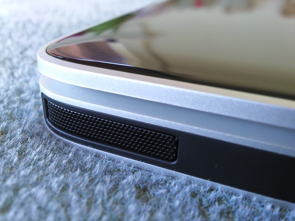
The machine has no cooling fan. Its aluminium body acts as a passive heatsink.
Main components
| Component | Part or model |
|---|---|
| System model | Nokia Booklet 3G NYU00 |
| Processor | Intel Atom Z530 |
| Chipset | Intel SCH US15W, AF82US15W |
| Graphics | Intel GMA 500, PowerVR SGX535 |
| Memory | 1 GB DDR2 SDRAM, soldered |
| Internal display | AU Optronics B101EW01 V1 |
| Storage | Toshiba MK1235GSL, 120 GB |
| Audio codec | Realtek ALC269Q-GR |
| Embedded controller | ENE KB926BFC0 |
| WiFi | Qualcomm Atheros AR928X, reported ID 168c:002a |
| Bluetooth | CSR USB module |
| 3G modem | Option GTM382 |
| Webcam | Microdia, USB ID 0c45:6409 |
Sources and test methods
Several sources describe this machine; they do not all provide the same type of information.
Rime output
Rime provides its own versions of hardware discovery utilities. The lspci -v and lsusb -v output in this document comes from Rime, not Linux.
Rime also provides utilities for embedded controller access, hardware monitoring, and direct register tests.
These results record what Rime found on the tested machine. They include PCI identifiers, USB descriptors, register values, and the results of hardware operations.
Linux output
The following reports come from Linux:
| Command or source | Purpose |
|---|---|
dmidecode | Reads SMBIOS and DMI tables. |
cat /proc/cpuinfo | Reports processor details and features. |
lscpu | Reports processor topology, caches, address sizes, and frequencies. |
inxi | Summarises the system, drivers, battery, and sensors. |
edid-decode | Decodes the internal display's EDID. |
smartctl -i /dev/sda | Reports drive identification and SMART support. |
hdparm -I /dev/sda | Reports ATA device capabilities. |
hdparm --direct -t | Measures direct read speed. |
The Linux examples include a 5.10.0-11-686-pae kernel and a local build of smartmontools 7.2. Other software and kernel versions can report different driver states and CPU frequencies.
Firmware and hardware identification
BIOS
The machine uses Nokia BIOS version 2.00.T01, dated 03/05/2010. The BIOS occupies a 1 MB region of the shared 8 MB SPI flash.
The BIOS is based on Intel's Poulsbo reference firmware. Several OEM fields still contain reference platform data or placeholder strings.
The Linux dmidecode report identifies the system as follows:
| SMBIOS field | Reported value |
|---|---|
| BIOS vendor | Nokia |
| BIOS version | 2.00.T01 |
| BIOS release date | 03/05/2010 |
| BIOS ROM size | 1 MB |
| BIOS runtime size | 102880 bytes |
| BIOS revision | 49.49 |
| Firmware revision | 49.49 |
| System manufacturer | Nokia |
| Product name | Nokia Booklet 3G |
| System version | 00000000000000000000000000000040 |
| Baseboard manufacturer | Nokia |
| Baseboard product | NYU00 |
| Baseboard version | REFERENCE |
| Baseboard serial | INVALID |
| System family | ABCDEFGHIJKLMNOPQRSTUVWXYZ |
The OEM string table contains:
This is the Intel Poulsbo
Chipset CEB Platform
These values describe the reference platform where Nokia did not replace them with machine specific data.
Incorrect firmware declarations
Several SMBIOS entries conflict with the hardware observed on the machine.
- SMBIOS declares a fan, but the machine has no fan.
- The CPU maximum speed is reported as 2666 MHz, while the Atom Z530 has a maximum frequency of 1600 MHz.
- The HD Audio device is marked as disabled, although the audio hardware works.
- The memory device is described as a SODIMM at locator
DIMM0 J6D1, although the memory is soldered to the main board. - The baseboard version is
REFERENCE, and the serial field isINVALID.
The ACPI description of the embedded controller names 173 registers. The machine uses only part of this register space. The schematics also list components that are not fitted.
Firmware tables and schematics can provide register names and addresses. They do not prove that a device is present or connected. A read on the machine is needed to establish that.
Firmware fields that agree with the machine
Some firmware data agrees with the tested hardware.
- The processor has one physical core and two logical threads.
- The memory table reports 1 GB installed.
- The memory array's reported maximum capacity is also 1 GB.
- The memory map covers the range
0x00000000to0x3FFFFFFF. - The BIOS version is Nokia 2.00.T01.
The configured memory capacity agrees with the chipset limit, the SMBIOS memory location does not agree with the physical board.
Processor
The Booklet 3G uses the Intel Atom Z530, codenamed Silverthorne. It is based on the Bonnell microarchitecture and uses a 45 nm manufacturing process.
Specifications
| Property | Value |
|---|---|
| Model | Intel Atom Z530 |
| Codename | Silverthorne |
| Microarchitecture | Bonnell |
| Manufacturing process | 45 nm |
| Base frequency | 1.60 GHz |
| SpeedStep range | 800 MHz to 1.60 GHz |
| Front side bus | 533 MT/s |
| Bus base frequency | 133 MHz |
| L1 instruction cache | 32 KB |
| L1 data cache | 24 KB |
| L2 cache | 512 KB, shared by both threads |
| Physical cores | 1 |
| Logical threads | 2 |
| Thermal design power | 2 W |
| Average idle power | 220 mW |
| Transistor count | 47 million |
| Die area | 26 mm² |
| Package | 437 pin FCBGA |
| Instruction sets | MMX, SSE, SSE2, SSE3, SSSE3 |
| Other features | XD bit, Intel VT-x, EIST |
The front side bus transfers data at 533 MT/s from a base clock of 133 MHz.
The processor supports 32 bit virtual addressing. PAE provides an extended physical address format. The platform has only 1 GB of memory.
The Linux reports list the processor as family 6, model 28, stepping 2. The reported microcode revision is 0x211.
Processor topology and frequency
Linux reports two online logical CPUs, both have physical ID 0 and core ID 0. The processor has one physical core and two logical threads.
The recorded CPU frequencies differ between reports because the processor uses SpeedStep.
| Source | Reported frequency |
|---|---|
/proc/cpuinfo, logical CPU 0 | 903.241 MHz |
/proc/cpuinfo, logical CPU 1 | 949.179 MHz |
lscpu | 797.986 MHz |
inxi | 798 MHz |
lscpu, minimum | 800 MHz |
lscpu, maximum | 1600 MHz |
Linux reports these processor features:
fpu vme de pse tsc msr pae mce cx8 apic sep mtrr pge mca cmov pat
clflush dts acpi mmx fxsr sse sse2 ss ht tm pbe nx constant_tsc
arch_perfmon pebs bts cpuid aperfmperf pni dtes64 monitor ds_cpl
est tm2 ssse3 xtpr pdcm movbe lahf_lm dtherm
The processor reports no fdiv, f00f, or coma bug in /proc/cpuinfo.
The Linux lscpu report lists one core per socket, one socket, and two threads per core. It reports 24 KiB of L1 data cache, 32 KiB of L1 instruction cache, and 512 KiB of L2 cache.
Thermal monitoring
The processor has an internal digital thermal sensor. Rime reads it through the IA32_THERM_STATUS model specific register at 0x19C.
Bit 31 indicates whether the reading is valid. Bits 16 through 22 report the distance below the maximum junction temperature. For this processor, the configured TjMax value is 90 °C.
CPUID leaf 6, EAX bit 0, reports whether the digital thermal sensor is present. The Rime kernel checks this feature before reading the register. The related kernel feature is SYS_CPU_THERMAL.
The processor also provides external thermal diode pins, THRMDA and THRMDC. These connect to the EMC1402 temperature sensor.
Hardware thermal controls TM1 and TM2 reduce processor performance when the processor overheats.
Chipset
The Intel SCH US15W, part AF82US15W, is also known as Poulsbo. It combines most platform functions in one chip and connects to the Atom Z530 through the 533 MT/s front side bus.
Memory controller
The SCH contains a single channel DDR2 memory controller. It supports up to 1 GB of DDR2 533 memory.
The 1 GB capacity is the platform limit. The memory is soldered to the board.
Graphics
The SCH contains the Intel GMA 500 graphics controller. Its graphics core is the PowerVR SGX535 from Imagination Technologies.
The GMA 500 is not based on an Intel graphics core. This difference affects graphics driver development and support.
Other platform functions
The SCH provides the following functions:
- One EHCI USB 2.0 controller with eight ports.
- Three UHCI USB 1.1 companion controllers with two ports each.
- IDE and PATA storage control.
- SDIO and MMC control.
- HD Audio.
- One PCI Express 1.1 root port.
- An LPC bridge for the embedded controller and legacy interfaces.
- An SMBus host controller.
- ACPI 2.0 power management.
The USB controllers share their port assignments. The UHCI controllers handle slower devices connected through the EHCI port structure.
The IDE controller uses the chipset's PATA interface and a GL831 bridge connects it to the SATA drive.
The PCI Express root port connects to the Atheros WiFi card; the SDIO/MMC controller connects to the SD card slot.
The SCH SMBus host uses I/O base 0x1100. Its status register layout differs from the layout used by Intel ICH chipsets, and a driver must use the correct register definitions for the SCH.
The platform supports ACPI power states S3, S4, and S5. The embedded controller manages the machine's power sequence.
An external ICS 9UMS9610 clock generator is configured by the BIOS.
Memory
The Booklet 3G has 1 GB of DDR2 SDRAM soldered to the main board.
| Property | Value |
|---|---|
| Type | DDR2 SDRAM |
| Data rate | 533 MT/s |
| Standard | PC2-4200 |
| Capacity | 1 GB |
| Rank | Single rank |
| Channel configuration | Single channel |
| Data width | 32 bit |
| Address range | 0x00000000 to 0x3FFFFFFF |
| Memory controller | Intel SCH US15W |
| Memory chips | Hynix HY5PS1G1631CFP-S6 |
The memory chips sit beside the SCH. There is no memory socket or removable module.
SMBIOS reports a SODIMM at locator DIMM0 J6D1, with bank locator Bank 0. These strings come from the reference board and were not corrected for the Booklet.
The locator is a firmware label, not a physical location. The reported capacity and address range agree with the configured system.
The SMBIOS memory map also reports a partition width of 2. This field needs review against the single channel configuration described by the platform information.
Display and graphics
Graphics controller specifications
The GMA 500 uses the PowerVR SGX535 graphics core, from the Series 5 family.
| Property | Value |
|---|---|
| Controller | Intel GMA 500 |
| Graphics core | PowerVR SGX535, Series 5 |
| Shader architecture | Four unified shader pipelines |
| Core speed | 200 MHz |
| Shader speed | 200 MHz |
| Maximum shared memory in supplied specification | 1 GB |
| Graphics technology | 65 nm |
| DirectX | DirectX 9.0c, shader model 3.0 |
| Graphics features | OpenGL 2.0, PowerVR SGX kernel support, screen tiling, internal true colour processing, zero overhead antialiasing, 32 bit floating point operations |
| Reported announcement date | 2 March 2008 |
| Official driver | 8.14.10.2030, dated 16 September 2010 |
The feature list comes from the supplied graphics information. Support in a driver can depend on the operating system and driver version.
Hardware accelerated video decoding
The supplied GMA 500 specification lists the following video codec profiles.
| Codec | Profile | Reported level or limit |
|---|---|---|
| H.264 | Baseline | Level 3 |
| H.264 | Main | Level 4.1, up to 1080i at 30 fps or 1080p at 24 fps |
| H.264 | High | Level 4.1, up to 1080i at 30 fps or 1080p at 24 fps |
| MPEG-2 | Main | High |
| MPEG-4 | Simple | Level 3 |
| MPEG-4 | Advanced Simple | Level 5 |
| VC-1 | Simple | Medium |
| VC-1 | Advanced | Level 3, up to 1080i at 30 fps or 1080p at 24 fps |
| WMV9 | Simple | Medium |
| WMV9 | Main | High |
These entries describe the supplied hardware capability list, they do not establish that a specific operating system driver exposes every feature.
Internal panel
The internal display is an AU Optronics B101EW01 V1 panel.
| Property | Value |
|---|---|
| Size | 10.1 inch |
| Panel type | Si TFT LCD |
| Operating mode | TN, normally white |
| Surface | Antiglare |
| Native resolution | 1280 × 720 |
| Aspect ratio | 16:9 |
| Pixel density | 145 PPI |
| Refresh rate | 60 Hz |
| Colour depth | 262K colours, 6 bit with dithering |
| Panel interface | Single channel LVDS, 6 bit |
| Connector | JP3, 30 pin |
| Pixel clock | 61.500 MHz |
| Backlight | White LED |
| Brightness | 180 cd/m² |
| Contrast ratio | 500:1 |
| Rise time | 12 ms |
| Fall time | 4 ms |
| Operating temperature | 0 to 50 °C |
EDID data
Linux's edid-decode utility reads the EDID from /sys/class/drm/card0-LVDS-1/edid.
The report identifies the panel as follows:
| Property | Reported value |
|---|---|
| EDID version | 1.3 |
| Manufacturer | AUO |
| Model number | 4565 |
| Manufacture date | Week 1 of 2009 |
| Physical image size | 222 × 125 mm |
| Gamma | 2.20 |
| Colour mode | RGB |
| Preferred timing | 1280 × 720 at 60.029 Hz |
| Horizontal frequency | 44.181 kHz |
| Pixel clock | 61.500 MHz |
| EDID checksum | 0xC3 |
The detailed timing descriptor reports these intervals:
| Timing | Value |
|---|---|
| Horizontal front porch | 48 pixels |
| Horizontal sync | 32 pixels |
| Horizontal back porch | 32 pixels |
| Horizontal sync polarity | Negative |
| Vertical front porch | 3 lines |
| Vertical sync | 6 lines |
| Vertical back porch | 7 lines |
| Vertical sync polarity | Negative |
The EDID contains the preferred 1280 × 720 mode; it has no established or standard timings.
Native display mode
The VBIOS does not set the native resolution as a direct source mode. It configures pipe B with panel timing totals of 1392 × 736 and uses the panel fitter to scale a smaller source.
A read only probe on the machine confirmed the following state:
- The internal panel uses pipe B.
- The pipe total timing is 1392 × 736.
- The source is 800 × 600.
- The panel fitter scales the source to the panel.
VBE offers 800 × 600 and 1024 × 768. Native 1280 × 720 requires a different mode setting procedure.
The known procedure changes these registers:
- Plane source size, stride, and position.
- Pipe source size.
- Panel fitter configuration.
The procedure leaves the pipe and PLL configuration unchanged and turns the panel fitter off; it does not write to the DPLL, LVDS port, or display power sequencer.
This procedure comes from tests on the machine, any change to display initialization should preserve the existing pipe, PLL, LVDS, and power sequence state.
Backlight control
The backlight uses the GMA 500 PWM register BLC_PWM_CTL at 0x61254.
The PWM period is stored in bits 17 through 31. The period value is doubled, and the duty value is stored in the low 16 bits and is even.
The firmware configures the period, while software changes the duty value.
Panel power
The panel power sequencer is controlled through PP_CONTROL at 0x61204.
Bit 0 selects the panel power target state. PP_STATUS at 0x61200, bit 31, reports whether the panel is on.
Rime's display server turns the backlight off before clearing the panel power target. It turns the backlight on after the panel has powered up. This follows the sequence used by the Linux gma500 driver.
Turning the panel off as part of an idle clock operation would require one sequencer write, but this has not yet been tested on the Booklet.
HDMI output
The HDMI transmitter is a Silicon Image SiI1392CNU, also known as VastLane; it connects to the main board at JP5.
| Property | Value |
|---|---|
| Transmitter | Silicon Image SiI1392CNU |
| Board connector | JP5 |
| Maximum stated mode | 1920 × 1080 at 60 Hz |
| Input | GMA 500 SDVO |
| Output | TMDS to HDMI |
| GMBus port | GPIOE |
| I2C address | 0x38 |
The VBIOS configures the transmitter during startup.
If an HDMI cable is present at boot, the VBIOS switches the output to HDMI and turns off the internal panel.
The VGA GMBus port, GPIOA, is unused because the Booklet has no VGA connector.
Storage
The internal drive connects through the SCH IDE controller and a GL831 PATA to SATA bridge.
The chain is:
Intel SCH IDE controller
        |
        |
Genesys Logic GL831 bridge
        |
        |
Toshiba MK1235GSL SATA drive
IDE controller
The IDE controller is PCI function 00:1f.1, with device ID 8086:811A.
| Property | Value |
|---|---|
| PCI function | 00:1f.1 |
| PCI class | 0x01 |
| PCI subclass | 0x01 |
| Primary IDE ports | 0x1F0 to 0x1F7 |
| Secondary IDE ports | 0x170 to 0x177 |
| Supported PIO modes | 0 to 4 |
| Supported UDMA modes | 0 to 5 |
| Bus master DMA | PCI BAR4 |
| Register compatibility | PIIX3 and PIIX4 |
The controller uses the usual ATA command and status registers, while bus master DMA uses PCI BAR4.
GL831 bridge
The Genesys Logic GL831 translates the PATA connection to SATA at 1.5 Gb/s.
The bridge is transparent to the host, it does not appear on the PCI bus, has no host accessible registers, and does not change the ATA command set.
The GL831 does not pass bus master DMA commands through to the drive, therefore a UDMA transfer through this bridge leaves the DMA engine active and never completes. Rime avoids this transfer mode.
Drive identification
The internal drive is a Toshiba MK1235GSL.
| Property | Value |
|---|---|
| Model | Toshiba MK1235GSL |
| Form factor | 1.8 inch |
| User capacity | 120,034,123,776 bytes, 120 GB |
| Linux device size | 111.79 GiB |
| LBA28 sector count | 234,441,648 |
| LBA48 sector count | 234,441,648 |
| Logical sector size | 512 bytes |
| Physical sector size | 512 bytes |
| Rotation speed | 4200 RPM |
| Cache | 8 MB |
| ATA standard reported by smartctl | ATA8-ACS |
| Transport speed | SATA at 1.5 Gb/s |
| SATA revision reported by smartctl | SATA 2.6 |
| Firmware | PV010A |
The sector count fits within LBA28 addressing. Linux reports that the drive is a non removable ATA device.
The hdparm -I output reports a queue depth of 32, an advanced power management level of 254, and a maximum multiple sector transfer count of 16. The current multiple sector transfer count is also 16.
The reported DMA modes are:
SDMA 0, 1, 2
MDMA 0, 1, 2
UDMA 0, 1, 2, 3, 4, 5
UDMA5 is marked as the current mode in the Linux report. This is the drive's reported capability. It does not show that the GL831 bridge can complete a bus master DMA transfer.
The hdparm -I output reports the transport as ATA8-AST, while smartctl reports ATA8-ACS.
SMART support
The Linux smartctl -i /dev/sda report was produced by smartmontools 7.2, dated 30 December 2020, on a local build using a Linux 5.10.0-11-686-pae kernel.
The report states:
- The drive is a Toshiba MK1235GSL.
- The firmware is PV010A.
- SMART capability is available.
- SMART is enabled.
- The drive is not in the smartmontools database used for this test.
The drive reports SMART support and responds to SMART commands, its health status is PASSED, and it reports 24 attributes.
The reported attribute IDs are:
1, 2, 3, 4, 5, 7, 8, 9, 10, 12, 191, 192, 193, 194,
196, 197, 198, 199, 222, 223, 224, 226, 229, 240
Attribute 194, Temperature_Celsius, stores three 16 bit values in its raw field:
- Current temperature.
- Lifetime minimum temperature.
- Lifetime maximum temperature.
A reading taken at 36 °C returned 36, 19, and 51. The first raw byte contains the current temperature.
A healthy unit provides the following baseline readings:
| Attribute | Meaning | Reported value |
|---|---|---|
| 1 | Raw read error rate | Normalised value 100, threshold 50 |
| 9 | Power on hours | 2732 |
| 198 | Offline uncorrectable sectors | 0 |
| 222 | Loaded hours | 1703 |
These values describe the tested unit, they are not expected values for every drive.
Storage command issues
Rime has found several problems with this storage path.
A SMART command that the channel refuses must not be sent again. The refusal can leave the request in the channel, and a later command can then stall the bus.
Writing to the drive select register while the BSY status bit is set is undefined. On the Booklet, this operation stalls the bus during the port read.
The GL831 bridge does not support the bus master DMA path used by the SCH IDE controller, and UDMA transfers through the bridge do not complete.
Read speed tests
The supplied Linux hdparm --direct -t results are:
| Label in the supplied notes | Device | Reported read speed |
|---|---|---|
| SSD test | /dev/sda1 | 60.30 MB/s |
| HDD test | /dev/sda1 | 38.29 MB/s |
| SD card test | /dev/mmcblk0p1 | 8.69 MB/s |
Audio
The HD Audio controller is PCI function 00:1b.0, with device ID 8086:811B. The controller connects to a Realtek ALC269Q-GR codec.
The audio hardware includes:
- Speaker and headphone DACs.
- Microphone ADCs.
- A class D speaker amplifier rated at 2.5 W per channel.
- A digital microphone input.
- Headphone and microphone jack detection.
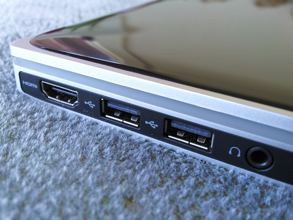
Two internal speakers connect to JP6 and are driven by the codec amplifier. A digital MEMS microphone is fitted in the top of the screen module, it connects to the codec's digital microphone input, using PDM.
The 3.5 mm combo jack is JP4; it supports headphones, a microphone, or a four pole headset.
The codec is controlled through the HD Audio bus with verb commands.
The firmware reports the HD Audio device as disabled, and this obviously conflicts with the working audio hardware observed on the machine.
Networking and connectivity
WiFi
The WiFi card is a Nokia branded Qualcomm Atheros OEM part. It is connected to PCI Express root port 00:1c.0 and appears as PCI function 02:00.0.
The reported PCI identifier is 168c:002a. This identifies the AR9280 PCI Express part. Other members of the AR9002 family include the AR9285, ID 168c:002b, and AR9287, ID 168c:002e.
The silicon version register at BAR0 offset 0x4020 identifies the fitted silicon.
The card supports 2.4 GHz 802.11b/g/n; two U.FL antenna connectors are populated, labelled MAIN and AUX, and the two antenna leads connect to the card.
The card uses calibration data in its own EEPROM; the driver reads this data through BAR0, using the address formula:
0x2000 + (word << 2)
The card does not need a firmware upload from the host; the firmware file path in the Linux driver belongs to USB devices in the wider product family. It is not required for this PCI Express card.
Bluetooth
The Bluetooth module is a CSR device connected to USB. Its USB ID is 0a12:0001. It operates at USB 1.1 full speed and is connected to the third UHCI controller, port 1.
WWAN modem
The Option GTM382, also known as Globetrotter MO40x, is connected through USB. Its USB ID is 0af0:7601. The modem is connected to EHCI port 4 and operates at USB 2.0 high speed.
The modem is described as a Qualcomm Gobi device, and it exposes several virtual USB interfaces for diagnostic access, GPS, GPS control, AT modem commands, and IP data.
The GPS requires UTC time after each power on. The SIM card connects at JP8.
USB Ethernet
The Booklet has no built in wired Ethernet controller or Ethernet connector.
Wireless coexistence
WiFi and Bluetooth both use the 2.4 GHz band; the board has no coexistence wire between the two devices. Any coordination must take place in software.
USB subsystem
The USB controllers are part of the Intel SCH US15W. The controller set contains one EHCI USB 2.0 controller with eight ports and three UHCI USB 1.1 companion controllers with two ports each.
The UHCI controllers handle slower devices connected through the EHCI port structure. The port and descriptor information in this section comes from Rime's lsusb -v, not Linux.
Port assignments
The Rime USB inventory reports these assignments:
| Port | Location or device | Connection |
|---|---|---|
| 1 | Left side | Empty |
| 2 | Left side | Empty |
| 3 | Right side | Empty |
| 4 | Internal modem slot | Option GTM382 modem |
| 5 | Internal Bluetooth module | CSR Bluetooth |
| 6 | Internal webcam | Microdia webcam |
| 7 | Not identified in the current inventory | Not reported |
| 8 | Not identified in the current inventory | Not reported |
The controller description lists eight EHCI ports, while the current device inventory names six. The assignments of ports 7 and 8 have not been confirmed, they might be internal or not connected.
UHCI controllers
| Controller | PCI function | Ports | EHCI ports handled |
|---|---|---|---|
| UHCI 1 | 00:1d.0 | 2 | 1 and 2 |
| UHCI 2 | 00:1d.1 | 2 | 3 and 4 |
| UHCI 3 | 00:1d.2 | 2 | 5 and 6 |
The companion controllers handle low speed and full speed devices. High speed devices use EHCI.
EHCI controller
The EHCI controller is PCI function 00:1d.7, with device ID 8086:8117; it supports USB 2.0 high speed and has eight ports; it hands slower devices to the three UHCI companion controllers.
Option GTM382 modem
The modem reports these identifiers:
| Property | Value |
|---|---|
| USB ID | 0af0:7601 |
| Version | 0.00 |
| Bus address in the captured Rime output | 3 |
| Speed | High speed |
| Device name | Option N.V. Globetrotter HSUPA Mode |
The device exposes ten interfaces; interfaces 0 through 8 are vendor specific, and each has one bulk input endpoint and one bulk output endpoint. These endpoints use 512 byte packets.
The endpoint mapping for these interfaces follows the interface number.
| Interface | Input endpoint | Output endpoint | Packet size |
|---|---|---|---|
| 0 | 1 | 1 | 512 bytes |
| 1 | 2 | 2 | 512 bytes |
| 2 | 3 | 3 | 512 bytes |
| 3 | 4 | 4 | 512 bytes |
| 4 | 5 | 5 | 512 bytes |
| 5 | 6 | 6 | 512 bytes |
| 6 | 7 | 7 | 512 bytes |
| 7 | 8 | 8 | 512 bytes |
| 8 | 9 | 9 | 512 bytes |
Interface 9 reports three endpoints:
- Endpoint 10 input, interrupt, 64 byte packets, every 2 ms.
- Endpoint 11 input, bulk, 512 byte packets.
- Endpoint 10 output, bulk, 512 byte packets.
The endpoint descriptions identify transfer types and packet sizes.
CSR Bluetooth module
The Bluetooth device reports these identifiers:
| Property | Value |
|---|---|
| USB ID | 0a12:0001 |
| Version | 52.76 |
| Bus address in the captured Rime output | 1 |
| Speed | Full speed |
Interface 0 provides interrupt and bulk endpoints.
- Endpoint 1 input, interrupt, 16 byte packets, every 1 ms.
- Endpoint 2 output, bulk, 64 byte packets.
- Endpoint 2 input, bulk, 64 byte packets.
Interface 1 provides isochronous input and output endpoints through endpoint 3. It has several alternate settings, which change the packet size.
| Alternate setting | Packet size | Interval |
|---|---|---|
| Default | 0 bytes | 1 ms |
| 1 | 9 bytes | 1 ms |
| 2 | 17 bytes | 1 ms |
| 3 | 25 bytes | 1 ms |
| 4 | 33 bytes | 1 ms |
| 5 | 49 bytes | 1 ms |
Microdia webcam
The webcam reports these identifiers:
| Property | Value |
|---|---|
| USB ID | 0c45:6409 |
| Version | 97.30 |
| Bus address in the captured Rime output | 4 |
| Speed | High speed |
| Device name | Sonix Technolog USB 2.0 Camera |
The webcam exposes two video interfaces.
Interface 0 uses endpoint 3 for interrupt input; it transfers 16 byte packets every 4 ms.
Interface 1 uses endpoint 1 for isochronous input. Rime reports six alternate settings.
| Alternate setting | Packet size | Packets per frame | Interval |
|---|---|---|---|
| 1 | 128 bytes | 1 | 125 µs |
| 2 | 256 bytes | 1 | 125 µs |
| 3 | 800 bytes | 1 | 125 µs |
| 4 | 800 bytes | 2 | 125 µs |
| 5 | 800 bytes | 3 | 125 µs |
| 6 | 1024 bytes | 3 | 125 µs |
The captured descriptors do not identify the video format and resolution for each setting.
SDIO and MMC
The SDIO/MMC controller is PCI function 00:1e.0, with device ID 8086:811C. It is SDHCI compatible and connects to the SD card slot JP7 on the IO board.
The slot supports SD and SDHC cards, and it uses the native SD host controller in the SCH, not a USB card reader.
The BIOS does not expose the slot through INT 13h, so the SD slot is not bootable through the normal BIOS disk interface.
Linux identifies the card device in the supplied speed test as /dev/mmcblk0p1.
Embedded controller
The Booklet uses an ENE KB926BFC0 embedded controller; an 8051 based microcontroller that manages most low speed hardware and power functions.
The EC remains active when the host sleeps. It manages the keyboard, touchpad, LEDs, battery, charger, lid switch, temperature sensor, and system power sequence.
Controller specifications
| Property | Value |
|---|---|
| Controller | ENE KB926BFC0 |
| CPU core | 8051 |
| Clock options | 8, 16, or 22 MHz |
| Internal RAM | 128 bytes |
| Interrupt sources | 24 |
| Timers | Two 16 bit timers |
| UART | One |
| Package | 128 pin LQFP |
| Sleep modes | Idle and Stop |
| Stop mode clock | 32.768 kHz oscillator |
The EC firmware occupies 64 KB in two segments and was built with Keil C51.
The EC shares an 8 MB SPI flash with the system BIOS; the flash may be a cFeon EN25F80 or a Macronix MX25L8005. The X Bus arbiter shares access to the flash between the EC and the host.
Host interfaces
Host communicates with the EC through three standard interfaces and one additional interface used by Rime.
8042 keyboard controller
The 8042 interface uses I/O ports 0x60 and 0x64.
IRQ1 is used for the keyboard, and IRQ12 is used for the mouse. The EC emulates a standard 8042 in hardware; this interface carries keyboard and touchpad input.
ACPI embedded controller
The ACPI EC interface uses ports 0x62 and 0x66.
| Command | Function |
|---|---|
0x80 | Read |
0x81 | Write |
0x82 | Enable burst mode |
0x83 | Disable burst mode |
0x84 | Query |
This interface gives the host access to EC register space used for battery, temperature, brightness, and related functions.
SMBus slave
The EC appears as a slave at SMBus address 0x69 on the SCH SMBus.
A scan of the SCH SMBus reports only this device: the temperature sensor, charger, and smart battery connect to the EC's own SMBus master. EC reads them and makes their data available to the host.
Index I/O
Rime's ec server uses the KB926 Index I/O window at ports 0xFF2D to 0xFF2F.
The host writes the address high byte, then the address low byte, and then accesses the data; this interface has no handshake.
The ACPI register space is in bank 0xF4. Bank 0xFC contains GPIO output data.
Bit 3 of register 0x2D in bank 0xFC is GPXIOA11. This signal controls the modem's 3G_EN# line. The EC sets the line according to the wireless key state and modem radio control.
Radio state
The radio state byte is at register 0xBB. This is the group of EC registers explained by the DSDT.
ANTR reads this byte, and ANTW writes its first two bits. The byte reports WLAN and Bluetooth power state, whether each device is fitted, the wireless kill switch state, and WLAN status.
The brightness keys generate ACPI query events 0x11 for brightness down and 0x12 for brightness up.
Keyboard and touchpad
The EC scans an 18 by 8 keyboard matrix, handles debounce and ghost key cancellation, and translates key presses to PS/2 Set 2 scancodes.
It also manages the Synaptics PS/2 touchpad. A pass through path to the 8042 supports low latency input.
LEDs
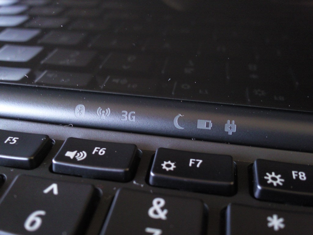
The EC controls the following indicators through GPIO:
- Power.
- WiFi.
- Bluetooth.
- Disk activity.
- Charging.
Temperature and analogue inputs
The EC reads the EMC1402 temperature sensor through its own SMBus master. Six 10 bit ADC channels monitor supply rails and thermistors.
The EC also contains a four channel, 8 bit DAC, six PWM channels, an RTC, and a watchdog. Two PWM channels are 8 bit, two are 14 bit, and two are unused fan channels.
The RTC uses a 32.768 kHz crystal. These EC internal functions are not host accessible registers.
Battery and charger
The EC communicates with the ISL6251 charger and the smart battery over its own SMBus master. It monitors the battery and supervises charging.
Power control
The EC controls transitions between S0, S3, S4, and S5.
Wake sources include the lid switch, power button, AC adapter, and RTC alarm.
The EC carries out the power sequence independently of the host CPU.
Sensors and monitoring
CPU temperature
The Atom Z530 contains an internal digital thermal sensor. Rime reads it through MSR 0x19C.
The kernel checks CPUID leaf 6, EAX bit 0, before reading the sensor. The value is valid when bit 31 of IA32_THERM_STATUS is set.
The reported thermal distance is stored in bits 16 through 22. The configured TjMax value is 90 °C.
External temperature sensor
The external temperature sensor is an SMSC EMC1402-1-ACZL. It has a stated accuracy of 1 °C and reads the CPU through its external thermal diode.
The sensor connects to the EC's SMBus master. The host does not access it directly through the SCH SMBus.
The reported I2C address is 0x4C or 0x4D. The address used by the fitted sensor should be confirmed by reading the EC configuration or testing the available interface.
Drive temperature
The Toshiba drive reports its temperature through SMART attribute 194, Temperature_Celsius.
The raw field contains current, minimum, and maximum temperature values. The first raw byte provides the current reading.
Absent sensors
The early schematics show a TAOS TSL2561 ambient light sensor and an NXP MMA7455 accelerometer. Neither component is fitted to the tested machine.
The Booklet has no automatic ambient brightness control and no fall protection based on an accelerometer.
Consumer infrared hardware is present inside the EC, but the relevant pins are not connected.
Power and battery
Battery
The battery pack contains four cells in series.
| Property | Value |
|---|---|
| Cell configuration | Four cells in series |
| Nominal voltage | 14.8 V |
| Maximum voltage | 16.8 V |
| Design capacity | 3840 mAh |
| Design energy | 56.8 Wh |
| Connector | PJP3, 5 pin |
Aged units may report capacities between 2000 and 2500 mAh.
The battery has a smart battery controller at SMBus address 0x16. The EC communicates with the controller and provides access to its data. Reported values include voltage, current, temperature, charge, capacity, and cycle count.
Charger and power input
The charger is a Renesas ISL6251 synchronous buck controller. The EC sets charge current and voltage over SMBus.
The AC adapter supplies approximately 19 V. The EC monitors its presence.
Power components
| Component | Function |
|---|---|
| MAX8796G | CPU voltage regulator, IMVP-6, VID controlled |
| ISL6251 | Battery charger |
| AO4466 | MOSFETs |
| APL3510 | USB power switch, EC controlled |
| LM358A | Amplifier |
| ICS 9UMS9610 | Clock generator, configured by BIOS |
These components do not all provide a direct host interface. Several are controlled by the EC or BIOS.
Power states
The platform supports these ACPI states:
| State | Meaning |
|---|---|
| S0 | Working |
| S3 | Suspend to RAM |
| S4 | Hibernate |
| S5 | Soft off |
The EC manages the transition sequence for each state.
The measured power figures are approximately 5 to 7 W at idle and 8 to 10 W under load. The actual values depend on the battery, display brightness, wireless activity, and workload.
The aluminium body acts as a passive heatsink. The machine has no fan.
The Linux inxi snapshot reports a battery charge of 20.3 Wh and a condition of 20.3 Wh out of 56.8 Wh, or 36 percent.
Input devices
Keyboard
The keyboard connects to the main board at JP10. It uses an 18 by 8 matrix scanned by the EC.
The EC translates key presses to PS/2 Set 2 scancodes and sends them through port 0x60, with IRQ1.
The keyboard supports function keys, multimedia keys, and Fn combinations. The EC handles many Fn actions, including brightness control. These actions do not reach the host as ordinary key presses.
The 8042 handles the keyboard LED command 0xED, typematic rate, enable, and reset.
Scancode translation
The EC sends Set 2 scancodes. The 8042 translation bit converts them to Set 1.
The host must use one translation method at a time:
- Enable the 8042 translation bit and use Set 2 input from the EC.
- Or disable translation and command the keyboard into Set 1 with
0xF0 0x01.
Using both methods corrupts key input.
Num Lock and the Fn keypad
Num Lock defaults to off. The keyboard has no numeric keypad.
Some EC firmware versions from this period enable the Fn keypad overlay when the host turns on the Num Lock LED. With Num Lock off, the affected scancodes act as navigation keys.
The behavior should be checked against the EC firmware in the tested machine.
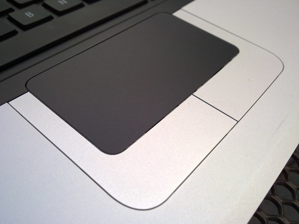
Touchpad
The touchpad is a Synaptics PS/2 device connected at JP11. It uses IRQ12 through the EC.
Standard PS/2 mouse operation works for pointer movement and both buttons.
An IntelliMouse sample rate sequence may enable a wheel mode, but the response of this touchpad has not been confirmed on the machine.
Synaptics extended features need Synaptics commands and are not currently used by Rime.
Other input devices
The power button and lid switch connect to the EC. The EC controls their behavior and uses them as inputs to the power state logic.
External USB keyboards and mice work through the USB stack.
The Booklet has no external PS/2 connector.
Board layout and connectors
The Booklet uses two boards connected by an 80 pin ribbon cable. The division between the two boards is transparent to software.
Main board
The main board is Compal LA-5301P. The supplied schematic is named LA-5301P Rev 0.2, while the board description identifies revision 1.0. These revision labels should be checked against the physical board and schematic files.
The main board contains:
- CPU and Intel SCH US15W.
- Memory.
- Embedded controller.
- BIOS flash.
- Audio codec.
- HDMI transmitter.
- GL831 storage bridge.
- Clock generator.
- EMC1402 temperature sensor.
- Voltage regulators.
- Most internal connectors.
IO board
The IO board is LS-5301P Rev 1A.
It contains:
- Mini PCI Express slots.
- SD card slot JP7.
- SIM slot JP8.
- External USB port JP9.
- Battery connector PJP3.
- Power input PJP1.
- ISL6251 charger.
The 1.8 inch drive sits between the boards, above the ribbon cable.
Main board connectors
| Connector | Function |
|---|---|
| JP1 | External USB |
| JP2 | External USB |
| JP3 | LCD LVDS panel |
| JP4 | Headphone and microphone combo jack |
| JP5 | HDMI |
| JP6 | Internal speakers |
| JP9 | Six pin header, purpose unknown |
| JP10 | Keyboard |
| JP11 | Touchpad |
| JP15 | Bluetooth |
| JP19 | Webcam and microphone module |
| JP20 | Internal drive |
| JP23 | Ribbon cable to IO board |
IO board connectors
| Connector | Function |
|---|---|
| JP3 | Ribbon cable to main board |
| JP4 | Six pin header, purpose unknown |
| JP5 | Half height mini PCI Express slot, WWAN over USB |
| JP6 | Full height mini PCI Express slot, WiFi over PCI Express |
| JP7 | SD card slot |
| JP8 | SIM card slot |
| JP9 | External USB |
| PJP1 | Power input |
| PJP3 | Battery |
The unknown six pin headers JP9 on the main board and JP4 on the IO board are not required for normal operation.
PCI device reference
Rime's lspci -v utility reports 12 PCI functions on the tested machine. Eleven are Intel SCH functions, and one is the Atheros WiFi card.
Device list
| PCI address | Device | Vendor and device ID | Class and subclass |
|---|---|---|---|
00:00.0 | Intel SCH US15W host bridge | 8086:8100 | 06:00 |
00:02.0 | Intel GMA 500 graphics | 8086:8108 | 03:00 |
00:1b.0 | Intel SCH HD Audio | 8086:811B | 04:03 |
00:1c.0 | Intel SCH PCI Express port 1 | 8086:8110 | 06:04 |
00:1d.0 | Intel SCH UHCI 1 | 8086:8114 | 0C:03 |
00:1d.1 | Intel SCH UHCI 2 | 8086:8115 | 0C:03 |
00:1d.2 | Intel SCH UHCI 3 | 8086:8116 | 0C:03 |
00:1d.7 | Intel SCH EHCI | 8086:8117 | 0C:03 |
00:1e.0 | Intel SCH SDIO/MMC | 8086:811C | 08:05 |
00:1f.0 | Intel SCH LPC bridge | 8086:8119 | 06:01 |
00:1f.1 | Intel SCH IDE controller | 8086:811A | 01:01 |
02:00.0 | Qualcomm Atheros AR928X WiFi | 168C:002A | 02:80 |
The PCI class field lists the base class and subclass. Where reported, the programming interface distinguishes UHCI from EHCI.
The WiFi card is behind the PCI Express bridge at 00:1c.0. The bridge reports secondary bus 2.
Common PCI settings
The Rime report gives revision 07 and subsystem ID 13b8:0001 for the SCH functions that report these fields. The Atheros card reports subsystem ID 1113:d822.
The reported PCI status for the SCH functions has no detected errors. The SCH device functions use memory, I/O, or both as shown in the following resource tables.
Host bridge
The Intel SCH US15W host bridge has device ID 8086:8100.
Rime reports no interrupt, no BARs, no PCI capabilities, and no detected errors for this function. It enables memory and I/O decoding and bus mastering. The reported header type is 0.
Graphics controller
The GMA 500 has device ID 8086:8108.
BAR0 contains the graphics registers and the framebuffer.
| BAR | Type | Address | Size | Width |
|---|---|---|---|---|
| BAR0 | Memory | 0xD0100000 | 512 KB | 32 bit |
| BAR1 | I/O | 0x1800 | 8 ports | Not applicable |
| BAR2 | Memory | 0xC0000000 | 256 MB | 32 bit |
| BAR3 | Memory | 0xD0180000 | 256 KB | 32 bit |
Rime reports interrupt pin A, IRQ 7. Memory and I/O decoding and bus mastering are enabled. INTx interrupts are allowed, and no parity or system error is reported.
The function reports power management, vendor specific, and MSI capabilities. It is in D0 and can sleep in D3. PME wake is not supported. MSI is off, with one vector and a 32 bit address.
HD Audio controller
The HD Audio controller has device ID 8086:811B.
BAR0 is a 64 bit memory BAR at 0xD01C0000, with a size of 16 KB. The controller connects to the Realtek ALC269 codec.
Rime reports interrupt pin A, IRQ 10. Memory decoding and bus mastering are enabled. I/O decoding is off. INTx interrupts are allowed, and no parity or system error is reported.
The function reports power management and PCI Express capabilities. It is in D0 and can sleep in D3. The PCI Express endpoint reports an unknown link speed of 0. The reported ASPM state is L0s, with a maximum payload of 128 bytes and a read request size of 128 bytes.
PCI Express root port
PCI function 00:1c.0 has device ID 8086:8110.
It is a PCI Express root port with a reported link speed of 2.5 GT/s at one lane. It connects to the Atheros WiFi card on secondary bus 2.
Rime reports interrupt pin A, IRQ 11. Memory and I/O decoding and bus mastering are enabled. The bridge has no BARs. Its header type is 1, and the output marks the function as multifunction.
The reported capabilities include PCI Express, bridge subsystem ID, and power management. The port is in D0 and can sleep in D3. PME wake is off. ASPM is L1, with a payload size of 128 bytes and a read request size of 128 bytes.
USB controllers
The three UHCI controllers and one EHCI controller are at:
00:1d.0, UHCI 1.00:1d.1, UHCI 2.00:1d.2, UHCI 3.00:1d.7, EHCI.
The UHCI controllers use I/O BAR4.
| PCI function | Controller | BAR | Address | Size | Interrupt |
|---|---|---|---|---|---|
00:1d.0 | UHCI 1 | BAR4 | 0x1820 | 32 ports of I/O space | Pin A, IRQ 10 |
00:1d.1 | UHCI 2 | BAR4 | 0x1840 | 32 ports of I/O space | Pin B, IRQ 5 |
00:1d.2 | UHCI 3 | BAR4 | 0x1860 | 32 ports of I/O space | Pin C, IRQ 3 |
The UHCI functions report no PCI capabilities. They use I/O space and bus mastering. INTx interrupts are allowed.
The EHCI controller uses a 1 KB memory BAR.
| Property | Value |
|---|---|
| PCI function | 00:1d.7 |
| Device ID | 8086:8117 |
| BAR0 | Memory at 0xD03C4000 |
| BAR0 size | 1 KB |
| BAR width | 32 bit |
| Interrupt | Pin D, IRQ 11 |
| Capabilities | Power management, debug port |
The EHCI function is in D0 and can sleep in D3. PME wake is off.
SDIO/MMC controller
The SDIO/MMC controller has device ID 8086:811C.
BAR0 is a 256 byte memory region at 0xD03C4400, 32 bit. Rime reports interrupt pin A, IRQ 10.
The controller connects to the SD card slot. It enables memory decoding and bus mastering. I/O decoding is off.
LPC bridge
The LPC bridge has device ID 8086:8119.
It provides access to the embedded controller, keyboard interface, BIOS flash, and legacy interfaces. Rime reports no BARs and no interrupt for this function. Bus mastering is off.
IDE controller
The IDE controller has device ID 8086:811A.
It is at PCI function 00:1f.1. Rime reports I/O decoding and bus mastering enabled, with memory decoding off. The function has no interrupt in the captured report.
BAR4 is an I/O region at 0x1810, with a size of 16 ports.
Atheros WiFi card
The Atheros card appears at 02:00.0, behind the SCH PCI Express root port.
| Property | Value |
|---|---|
| Vendor and device ID | 168C:002A |
| Subsystem ID | 1113:D822 |
| Revision | 01 |
| BAR0 | 64 KB memory at 0xD0000000 |
| Interrupt | Pin A, IRQ 7 |
| Capabilities | Power management, MSI, PCI Express, MSI-X |
| PCI Express link | 2.5 GT/s, one lane |
| ASPM | L1 |
| Maximum payload | 128 bytes |
| Read request size | 512 bytes |
Memory and I/O decoding and bus mastering are enabled. The device is in D0 and can sleep in D1 or D3. PME wake is off.
Rime reports MSI and MSI-X disabled. One vector is available in each report.
Disabled chipset functions
The SCH datasheet names additional functions, including PCIe port 2 with ID 8112 and SDIO functions with IDs 811D and 811E. The Booklet does not enable these functions.
SMBus and GMBus
The machine has two distinct host access paths for low speed devices: the SCH SMBus controller and the GMA 500 GMBus interfaces.
SCH SMBus
The SCH SMBus host controller uses I/O base 0x1100 and supports SMBus 2.0.
Its status register layout differs from the layout used by Intel ICH chipsets. Reusing the ICH status definitions causes status bits to be interpreted incorrectly.
A scan of the SCH SMBus finds one device: the EC at address 0x69.
The temperature sensor, charger, and smart battery connect to the EC's own SMBus master. The host reads their data through the EC.
The EC's SMBus master may also connect to the clock generator. This connection requires confirmation.
EC SMBus master
The known devices on the EC's SMBus master include:
| Address | Device | Host access |
|---|---|---|
0x16 | Smart battery | Through EC |
0x4C or 0x4D | EMC1402 temperature sensor | Through EC |
| Unknown | ISL6251 charger | Through EC |
| Possible | ICS 9UMS9610 clock generator | Connection unconfirmed |
The addresses listed here belong to the EC's SMBus master, not the SCH host controller.
GMA 500 GMBus
The GMA 500 provides I2C buses through its graphics registers. These buses are known as GMBus.
| Port | Signal | Device | Address |
|---|---|---|---|
| Panel | GPIOC | Panel EDID | 0x50 |
| SDVO or HDMI | GPIOE | SiI1392 HDMI transmitter | 0x38 |
| VGA | GPIOA | Unused | None |
GPIOA is unused because the Booklet has no VGA connector.
I/O ports and register addresses
I/O ports
| Address or range | Function |
|---|---|
0x60, 0x64 | 8042 keyboard controller |
0x62, 0x66 | ACPI embedded controller |
0x70, 0x71 | Real time clock |
0x170 to 0x177 | Secondary IDE |
0x1F0 to 0x1F7 | Primary IDE |
0x3F8 to 0x3FF | COM1 address range, no device responds |
0x1100 | SCH SMBus host base |
0xFF2D to 0xFF2F | EC Index I/O window |
The COM1 address range is decoded, but no device responds. The Booklet has no serial or parallel port.
Graphics registers
| Address | Register or function |
|---|---|
0x61200 | PP_STATUS |
0x61204 | PP_CONTROL |
0x61254 | BLC_PWM_CTL |
The panel power status is in bit 31 of PP_STATUS. Bit 0 of PP_CONTROL selects the panel power target state.
The backlight PWM period and duty values are in BLC_PWM_CTL.
SMBus and I2C addresses
| Address | Device | Bus |
|---|---|---|
0x16 | Smart battery | EC SMBus master |
0x38 | SiI1392 HDMI transmitter | GMA 500 GMBus, GPIOE |
0x4C or 0x4D | EMC1402 temperature sensor | EC SMBus master |
0x50 | Panel EDID | GMA 500 GMBus, GPIOC |
0x69 | Embedded controller | SCH SMBus |
Linux hardware reports
This section records information from Linux utilities. It does not describe output from Rime's lspci -v or lsusb -v.
dmidecode
The captured report identifies SMBIOS version 2.5, with 28 structures occupying 1009 bytes. The table starts at physical address 0x000DC010.
The BIOS structure reports vendor Nokia, version 2.00.T01, release date 03/05/2010, runtime size 102880 bytes, and ROM size 1 MB.
The system structure reports manufacturer Nokia and product name Nokia Booklet 3G. Its family string is ABCDEFGHIJKLMNOPQRSTUVWXYZ.
The baseboard structure reports manufacturer Nokia, product NYU00, version REFERENCE, and serial INVALID.
The processor structure reports:
- Manufacturer Intel.
- Processor ID bytes
C2 06 01 00 FF FB E9 BF. - Version C0.
- Reported voltage 1.2 V.
- Maximum speed 2666 MHz.
- Current speed 1600 MHz.
- One core and one enabled core.
- Two threads.
- Processor marked populated and enabled.
The reported upgrade method is ZIF Socket. This is another firmware field that should not be treated as a physical description of the soldered processor.
The cache structures report 64 KB for L1 and 512 KB for L2. The processor specific cache sizes are 32 KB instruction and 24 KB data for L1, and 512 KB for L2. The L1 cache size reported by SMBIOS does not match the sum of the processor's documented L1 caches.
The baseboard memory array structure reports system board memory, no error correction, maximum capacity 1 GB, and one device.
The memory device structure reports:
- Total width 32 bits.
- Data width 32 bits.
- Size 1 GB.
- Form factor SODIMM.
- Locator
DIMM0 J6D1. - Bank locator
Bank 0. - Type DDR2.
- Type detail Synchronous.
The memory mapped address structures cover 0x00000000 to 0x3FFFFFFF, with a size of 1 GB. One structure reports partition width 2.
The board and slot structures report two PCI Express slots. PCI Express Slot J7C1 is in use, and PCI Express Slot J8C1 is available.
The onboard device structure marks HD Audio as disabled. This conflicts with the working codec and audio path found on the machine.
Other DMI structures report the following:
| Structure | Reported information |
|---|---|
| Chassis | Manufacturer Nokia, type Portable |
| USB connector | External USB port entry |
| OEM strings | Intel Poulsbo and Chipset CEB Platform |
| System configuration | Jumper settings can be described here |
| System event log | Valid, not full; supports POST errors and ECC memory error events |
| System reset | Enabled; watchdog timer present |
| Power on password | Disabled |
| Administrator password | Disabled |
| Scheduled power on | 12-31 at 23:59:59 |
| Voltage probe | Processor location, status OK |
| Cooling device | Type Fan, status OK |
| Temperature probe | Processor location, status OK |
| Current probe | Processor location, status OK |
| Out of band remote access | Manufacturer Intel, inbound enabled, outbound disabled |
| System boot information | Status reported as out of specification |
The reported fan and cooling status do not agree with the physical machine, which has no fan. These fields are examples of reference firmware data that was not fully updated.
Serial numbers, the system UUID, and other identifying fields have been omitted.
/proc/cpuinfo
The Linux /proc/cpuinfo report identifies two logical CPUs. Both use vendor ID GenuineIntel and model name Intel(R) Atom(TM) CPU Z530 @ 1.60GHz.
Each entry reports:
- CPU family 6.
- Model 28.
- Stepping 2.
- Microcode
0x211. - Physical ID 0.
- One core.
- Two siblings.
- L2 cache size 512 KB.
- CLFLUSH size 64 bytes.
- Cache alignment 64 bytes.
- 32 bit physical and 32 bit virtual address sizes.
The flag list appears in the processor section.
The report lists no fdiv, f00f, or coma bug.
The recorded CPU frequencies were 903.241 MHz for logical CPU 0 and 949.179 MHz for logical CPU 1.
lscpu
The Linux lscpu report identifies an i686 system with 32 bit operation, little endian byte order, and two online CPUs.
| Property | Value |
|---|---|
| Architecture | i686 |
| CPU operation modes | 32 bit |
| Byte order | Little endian |
| Address sizes | 32 bit physical, 32 bit virtual |
| CPUs | 2 |
| Threads per core | 2 |
| Cores per socket | 1 |
| Sockets | 1 |
| CPU model | Intel Atom Z530 |
| Stepping | 2 |
| Minimum frequency | 800 MHz |
| Maximum frequency | 1600 MHz |
| Reported frequency | 797.986 MHz |
| BogoMIPS | 3191.94 |
| L1 data cache | 24 KiB |
| L1 instruction cache | 32 KiB |
| L2 cache | 512 KiB |
The report lists the processor as not affected by the following vulnerability checks: Itlb multihit, L1TF, MDS, Meltdown, Speculative Store Bypass, Spectre v1, Spectre v2, SRBDS, and TSX asynchronous abort. These are results from the supplied Linux environment, not a general guarantee for every operating system configuration.
inxi
The Linux inxi output provides a system summary.
| Area | Reported information |
|---|---|
| Machine | Nokia Booklet 3G, model NYU00 |
| BIOS | Nokia 2.00.T01, date 03/05/2010 |
| Battery | 20.3 Wh reported charge; 20.3 Wh out of 56.8 Wh, or 36 percent |
| CPU | Single core Atom Z530, two logical threads, L2 cache 512 KiB |
| CPU speed | 798 MHz, minimum 800 MHz, maximum 1600 MHz |
| Graphics | Intel US15W/US15X SCH graphics, driver reported as gma500 |
| Display | X.org 1.20.11, modesetting driver loaded |
| Audio | Intel SCH HD Audio, Linux driver snd_hda_intel |
| Network | Qualcomm Atheros AR928X, Linux driver ath9k |
| WWAN interface | hso0, reported down |
| Bluetooth | CSR USB device, driver btusb, reported down |
| Drive | Toshiba MK1235GSL, 111.79 GiB |
| Storage usage | 6.04 GiB used, 5.4 percent |
| CPU temperature | 33 °C |
| Motherboard temperature | Not available |
| Fan speed | Not available |
The reported network, Bluetooth, and driver states describe one Linux session. They do not establish the behavior of other operating systems.
EDID
The Linux edid-decode output identifies the panel manufacturer as AUO, model 4565, made in week 1 of 2009.
It reports the preferred mode as 1280 × 720 at 60.029 Hz, with a 61.500 MHz pixel clock and physical size of 222 × 125 mm.